
Lapping Powders for Chamfering and Edge Profiling of Optical Components
The chamfering process is generally divided into three stages: rough chamfering (edge creation, removal of chippings, and shaping) → intermediate/fine chamfering (controlling edge chipping and reducing the subsurface damage layer) → precision chamfering/polishing (final edge refinement prior to coating).
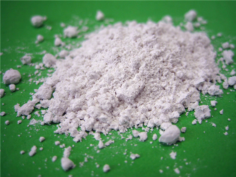
1. White Fused Alumina (WA) lapping powder
Applications: Chamfering and intermediate processing of soft optical glass, germanium crystals, calcium fluoride infrared windows, and crystals sensitive to iron contamination.
Advantages: Higher toughness compared to GC, resulting in a lower risk of edge chipping and reduced heat generation. Ideal for components where edge integrity is prioritized over extremely high material removal rates.
Normal Sizes: JIS#1500 #2000 #2500 #3000 #4000
Disadvantages: Lower cutting efficiency compared to Green Silicon Carbide (GC).
2. Green Silicon Carbide (GC) lapping Powder
Applications: Rough chamfering and edge profiling of fused silica, borosilicate glass, infrared optical crystals, and optical filter blanks.
Advantages: Sharp with self-sharpening properties, fast cutting rate, low magnetic impurity content, and controllable subsurface damage. Low-magnetic variants are suitable for optical components used in optical communications and quantum sensing.
Normal Sizes: #800 #1000 #1200 #1500 #2000
Disadvantages: Due to its high hardness, larger grit sizes of Green Silicon Carbide (GC) can easily cause minor edge chipping.

3. Diamond Lapping Powder
Applications: Chamfering and shaping of high-hardness optical components, such as sapphire, single-crystal silicon carbide, and YAG laser crystals.
Advantages: Exceptional hardness, high removal efficiency, and consistent grit sizing. Can be used in both bonded abrasive tools (grinding wheels) and as a loose abrasive slurry.
Normal Sizes: JIS #1500 #2000 #2500 #3000 #4000 #6000 #8000 #10000
Disadvantages: High cost; if process parameters are not strictly controlled, it can easily cause scratches on the optical side surfaces.
4. Black Silicon Carbide (C) Lapping Powder
Applications: Ordinary optical glass, lighting lenses, and chamfering of non-precision components.
Advantages: Cost-effective, fast cutting rate.
Disadvantages: Higher levels of impurities and magnetic particles; unsuitable for optical communications, quantum sensing, or precision-coated optical components.

5.Zirconium Silicate-Alumina Composite Lapping Powder (Equivalent to Japan’s FUJIMI FO lapping powder)
Applications: Used after rough chamfering but before final polishing; ideal for refining optical edges, smoothing chamfered surfaces, and reducing the time required for subsequent polishing steps.
Advantages: Combines soft and hard components, resulting in fewer scratches and uniform edge finishing. Widely used in optical cold-processing facilities for pre-lapping after chamfering. Note: Not intended for initial rough edge-shaping; material removal rate is relatively low.

In summary, the mainstream choices for rough shaping and chamfering of optical components are: Green Silicon Carbide (the preferred choice for precision optics), White Fused Alumina (for soft crystals and controlling edge chipping), and Black Silicon Carbide (an economical option). Diamond are used for ultra-hard crystals like sapphire, while Zirconium Silicate-Alumina composite lapping powder (Equivalent to Japan’s FUJIMI FO lapping powder) is used for intermediate-precision edge finishing and polishing.